|
LED Industry |
|
||||||||||||||||||||||
|
Reliability Testing |
|
Reliability Testing Service |
|
||||||||||
|
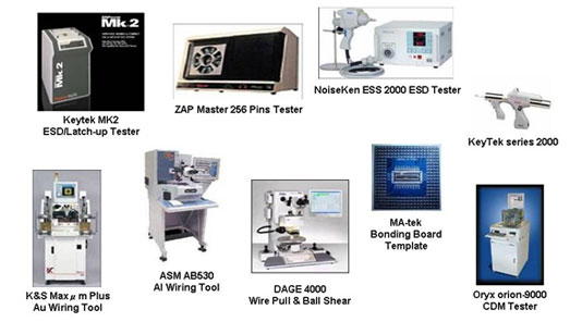
LED Reliability Testing Facilities |
 |
|
ESD, Latch-up, Testing/Wire Bonding |
 |
|
LED ESD Testing |
 |
|
X-ray Inspection |
|
X-ray Photography |
 |
|
X-ray lnspection of LED |
 |
|
Failure Analysis (FA) |
|
Thermal, EMMI/InGaAs,OBIRCH |
Defect Localization by EMMI/InGaAs, OBIRCH
 |
EMMI/InGaAs, OBIRCH for FA Application
 |
|
Texturing (Surface Morphology) |
|
Optical Profiler |
|
|
|


|
Texturing (Surface Morphology) |
 Surface morphology of LED die surface roughness after RIE etching or ion bombardment. |
|
|
Chip Structure and Film Thickness |
|
SEM, DB-FIB, TEM |

X-S view SEM |

|
|
Chip Structure and Film Thickness |
 Precise X-S view by DB-FIB |
|
 X-S view TEM |

(a)MQW and super lattice;(b)HR TEM of MQW;(c)PSS and buffer layer |
|
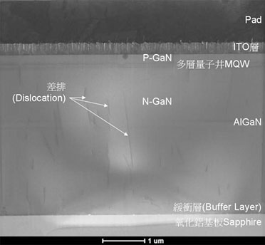
Crystalline Defects (Dislocations) |
|
X-S TEM, P-V TEM |

TEM Imaging (Dislocations in epitaxial butter layer) |
 X-S & P-V TEM at requested area to observe the dislocation density and its spatial distribution |
|
|
Depth Profiling of Elemental Analysis |
|
TEM/EDX, SIMS |
EM/EDX Line Profile – Blue LED – MQW and Superlattice
 In% in superlattice can be defected down to 0.2at% |
Elemental Depth profile by SIMS
 SIMS is also feasible now. |