FIB
|
Technical Concept |
|
Focused Ion Beam microscope(FIB) uses gallium(Ga)as a metal ion source, can be used for lithography by ion sputtering, deposition and etching for metal and oxide, and thus is a great tool for MEMS. |
Focused Ion Beam microscope (FIB) uses gallium (Ga) as a metal ion source, whose extreme low vapor pressor of 6.98×10-38 Torr is proper for various vacuum environments, even UHV. The system adds a strong electric field to melt and thus modify the shape of the metal source. Finally, the source holds a Taylor-cone shape whose apex is sharp enough to eject a beam of Ga ions. The beam with energy dispersion of 4.5 ev and brightness of 106 A/cm2.sr can be focused to an area smaller than 10 nm and is thus used for nano-lithography.
A FIB system consists of a liquid ion source, focusing and scanning lenses, a moving stage, a gas inlet system (GIS), and signal detectors. It can be used for lithography by ion sputtering, deposition and etching for metal and oxide, and thus is a great tool for MEMS.
A FIB system combined with an SEM is called as a dual-beam FIB. Such machines can be used for both non-destructive nano-inspection by its SEM mode and destructive nano-lithography by its FIB mode. It is powerful in precise nano-lithgoraphy of a selected local area. For example, it has been widely used for TEM sample preparation.
|
Applications |
- IC circuit repair
- Cross-sectional inspection on selected areas.
- Ion Channeling Contrast
- TEM sample preparation

A focused ion beam system. (a) liquid ion beam source (b) single beam system with GIS (gas of Br2、XeF2、TEOS) for circuit repair (c) Dual-beam FIB system |
|
Application Cases |
|
Case1.Circuit Editing |
The original design for developing ICs usually contains many mistakes to cause function error. Therefore a trial IC fabrication is needed for testing function accuracy. Incorrect IC circuit design is one of the most important reasons to cause error. Therefore a method to repair the circuit of trial ICs is needed for the development of ICs. With its great power on cutting, etching, and deposition for metals and oxides, FIB technology is inexpensive and efficient for circuit repair or editing.
A circuit editing can be performed in the front-side and back-side depending on the difference of packages and repaired areas.
- Front-side editing starts from topsides of IC chips and then processes lower layer by layer, as typically shown in Figure-2.
- Back-side editing starts from the backsides of IC chips (Si substrate) and then gradually processes to the upper area as typically shown in Figure-3.
In general, the difficulty of editing depends on circuit structures. Difficulty decreases with increasing area allowed to process. Processing upper layers are easier. Wires of copper are easier to edit than those of Al. The editing difficulty for the front side is lower than that for the back side. An editing process usually includes passivation or oxide removal, metal wire cutting, metal deposition, connecting wire deposition, metal pad deposition, oxide deposition, capacitor creation, and resistor fabrication.
Insulator deposition is caused by ion beam induced gas, such as TEOS or TMCTS, decomposition to form SiO2. There are two materials of W and Pt that can be selected for metal deposition. The former has lower resistance and better hole-filling power, but a lower deposition rate than the latter. The gas of C10H8 is used for carbon film deposition.
Aluminum can be etched by I2, Br2, or Cl2 while cooper can be removed by a combination of ion sputtering and water vapor. Insulator layers are etched by XeF2.
 |
(a) DecapsulationFigure-2.A typical case showing the process of front-side editing. (b) digging holes and filling metal (c) cutting and connecting wires (d) Deposited pt wire (e) cutting in M2 |
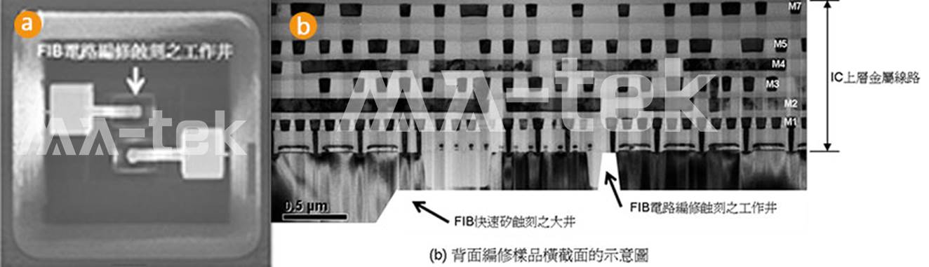 (a) Probing padsFigure-3.A typical example of back-side editing. (b) a typical cross-sectional image of a back-side-edited sample |
The circuit-editing for advanced IC circuits becomes more and more difficult because of continuously decreasing wire pitch. The difficulty can be overcome through the following three directions.
- Improving system quality, such as ion beam stability.
- Developing more powerful reactive gases for etching and deposition.
- Reducing charge accumulation.
|
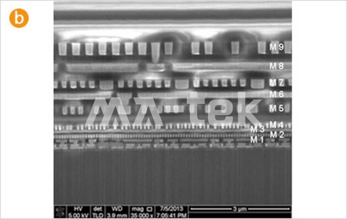
Case 2.Cross-sectional inspection |
FIB is allowed to create holes with precise location accuracy and thus is powerful to analyze failures inside samples. Such analysis usually exploits a dual-beam FIB system of which the FIB mode is used to cut through failures whose position and morphology image are provided by the SEM mode. For example, The image below typically shows how to obtain a cross-sectional IC image.

A schematic figure shows a typical process for a cross-sectional observation. |
An SEM mode image of a cross-sectional IC. |
|
Cases 3.Ion Channeling Contrast |
Many solid crystals have channel-like gaps along with specific crystalline directions. FIB systems are powerful enough to observe such gaps because their ion beams aligned and mis-aligned with gaps contribute clear image-contrast difference caused by distinct second electron and ion emissions. This phenomenon is called ion channeling contrast and its mechanism can be schematically explained by the following figure.
 |
A schematic figure shows the difference between ion beam aligned and misaligned channel directions.
Images of ion channeling contrast are powerful enough to clearly show stacking structures of different crystals and allow for analysis of grain size and direction. For example, the figure below shows cross-sectional images of a solder ball by optical microscopy (left) and FIB (right). The FIB image provides more information of Pb-Sn grain structure, caused by temperature difference between the PCB and IC in a binding process.
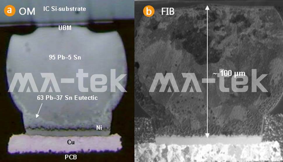 |
Cross-sectional images of a solder ball by (a) OM and (b) FIB
|
Case 4.TEM sample preparation (Pre-thin, Lift-out, Omni-probe) |
There are three FIB-based methods to prepare TEM samples:pre-thin, lift-out, and omni-probe.
 |
|
 |
|
 |
|
|
Contact |
|||||||||||
|
|
||||||||||
|
|
|||||||||||
|
|
||||||||||
|
|
|||||||||||
|
|