-
Electrical Property Measurement
-
PEM-CCD
-
PEM-InGaAs
-
OBIRCH
-
Thermal EMMI
-
C-AFM
-
AFM-based Nano-probing
-
SEM-based Nano-probing
-
EBIC / EBAC
-
EBIRCH
How can we help you? Get in touch with us
EBIC / EBAC
|
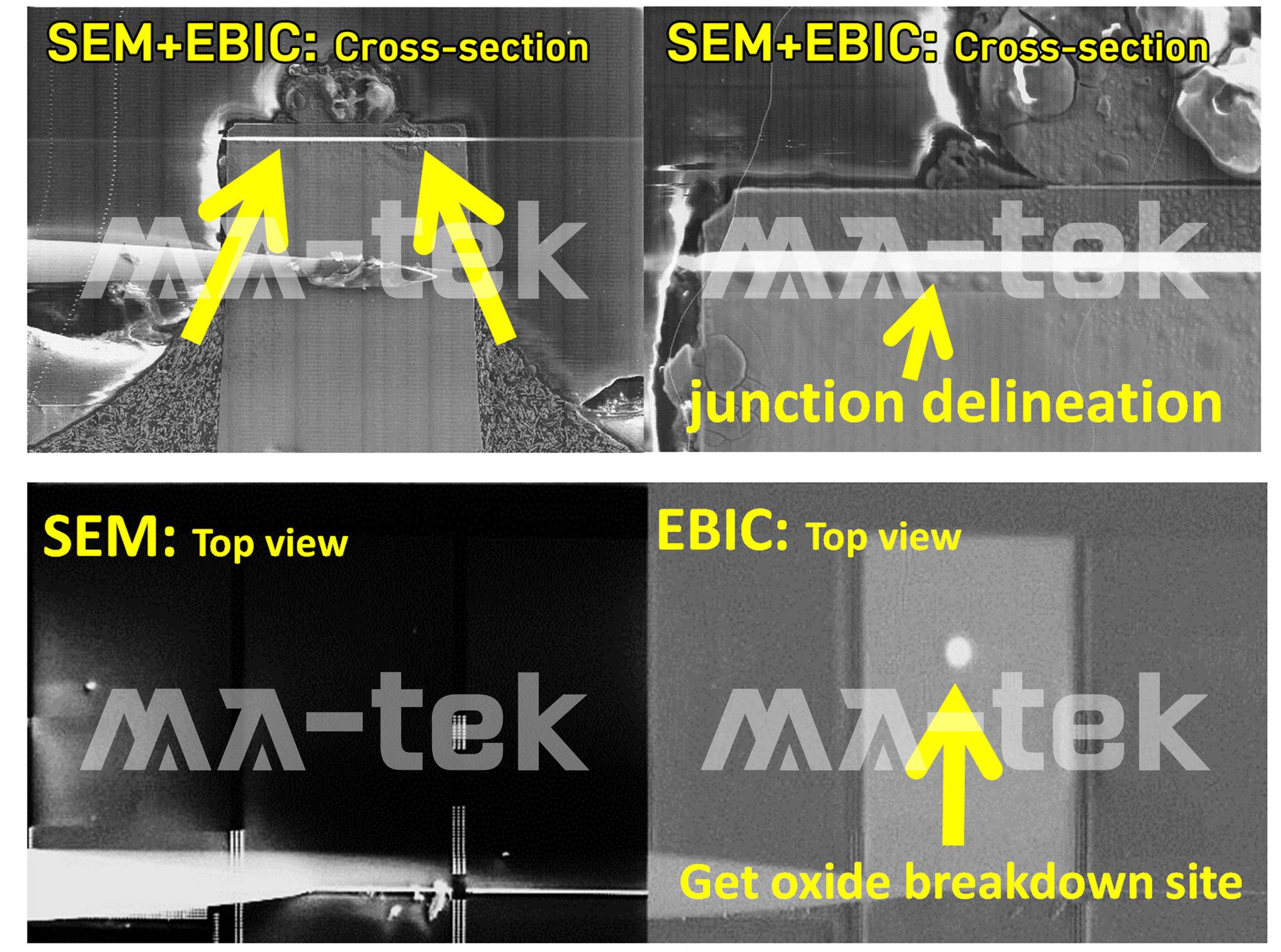
EBIC (Electron Beam Induced Current) |
|
EBIC is a method for imaging and characterization of p-n junctions, junction defects, and diffusion length. |
When an electron beam strikes a semiconductor, electro-hole pairs are generated and separated in the depletion region due to the built-in electric field, and a current flow can be measured.
|
|
|
|
EBAC (Electron Beam Absorbed Current) |
|
EBAC offers a quick and effective method to identify interconnect opens and shorts. |
EBAC utilizes the electron beam to penetrate the dielectric layers and inject charges inside the sample. The absorbed charges by the lower level metallization layer (3 or 4 layers deep) are measured by the current amplification through the probing probe.
|
|
|
|
Contact |
|||||||||||
|
|


